

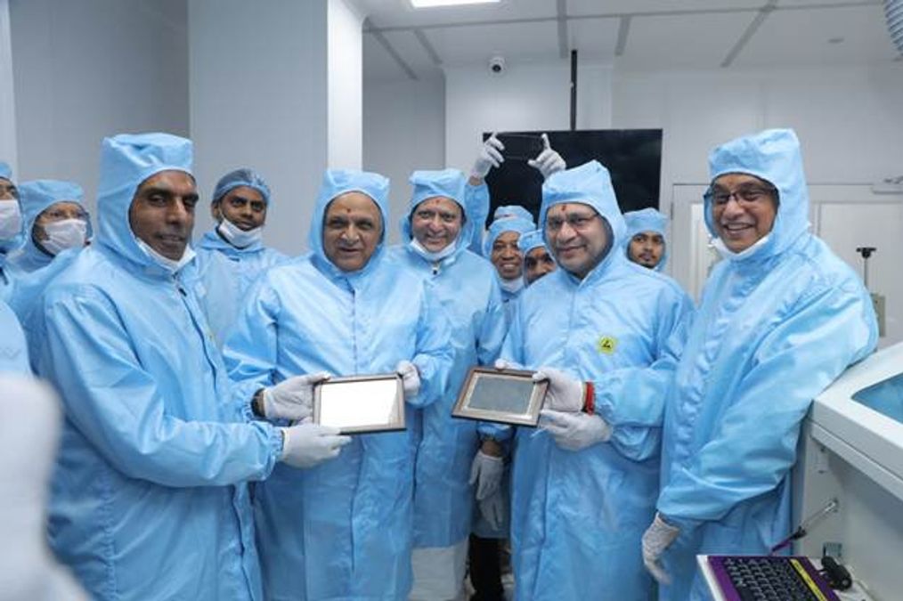
Union Minister of Electronics and Data Know-how, Ashwini Vaishnaw, together with Chief Minister of Gujarat, Bhupendra Patel, inaugurated one in every of India’s first end-to-end semiconductor OSAT pilot line facility of CG Energy at Sanand, Gujarat.
The ceremony marks a historic starting in India’s semiconductor journey below the visionary management of Prime Minister Narendra Modi.
The Minister mentioned that the inauguration of the pilot line represents a decisive step in fulfilling Bharat’s dream of growing semiconductor design, manufacturing, and downstream capabilities, with Gujarat rising as a pivotal hub on this transformation.
Vaishnaw underlined the essential position of the OSAT pilot line, noting that chips manufactured right here might be used for buyer qualification. As soon as these chips are accepted, it turns into a lot simpler for business crops to start full-scale manufacturing of certified merchandise. He emphasised that this inauguration is among the many most important milestones achieved below the India Semiconductor Mission, which has accepted 10 tasks thus far.
Highlighting the significance of growing a robust expertise base, the Minister mentioned that one of many main goals of the India Semiconductor Mission is to create a worldwide pipeline of expert professionals. By 2032, the world is projected to face a scarcity of 1 million semiconductor professionals, and India has the chance to bridge a major a part of this hole.
To this finish, the Authorities has partnered with 270 universities, and outfitted them with state-of-the-art semiconductor design instruments. In 2025 alone, these instruments recorded over 1.2 crore usages. As a direct consequence, 20 chips designed by 17 establishments have already been efficiently fabricated on the Semi-Conductor Laboratory (SCL), Mohali.
The Minister acknowledged that only a few international locations on the planet present college students with entry to such superior instruments. This initiative will empower India’s youth, strengthen the technical ecosystem, and place the nation as a worldwide hub of semiconductor expertise. He additionally acknowledged the robust assist of the Authorities of Gujarat and Chief Minister Bhupendra Patel in growing semiconductor ecosystem in Gujarat.
Chief Minister Bhupendra Patel lauded the initiative, highlighting its position in positioning the nation as a pacesetter in semiconductor design and manufacturing. The State Industries Minister, Balwant Singh Rajput. MLA Kanhubhai Patel, and senior officers of MeitY, and the management of CG Semi have been additionally current on the event.
CG Semi facility
The CG Semi facility at Sanand, Gujarat, is one in every of India’s first full-scale outsourced semiconductor meeting and check (OSAT) crops. It offers end-to-end options for chip meeting, packaging, testing and post-test providers, masking each conventional and superior packaging applied sciences. This marks a significant step in strengthening India’s semiconductor capabilities and supporting the nation’s purpose of changing into self-reliant whereas additionally serving world markets.
Backed by central and state authorities assist, CG Semi is investing over ₹7,600 crore (~USD 870 million) over 5 years to develop two state-of-the-art amenities (G1 and G2) in Sanand, Gujarat.
The G1 facility that was inaugurated. will function at a peak capability of roughly 0.5 million models per day. It’s outfitted to deal with end-to-end chip meeting, packaging, testing, and post-test providers. The ability options high-yield gear, a cutting-edge Manufacturing Execution System (MES) for Degree 1 automation and traceability, and in-house labs for reliability and failure evaluation. It’s presently present process ISO 9001 and IATF 16949 certification. Buyer qualification runs throughout varied packages will start following the inauguration. CG Semi is on observe to start business manufacturing in calendar 12 months 2026, as dedicated to ISM.
Positioned about 3 km from G1, the G2 facility is below development and anticipated to be accomplished by the tip of calendar 12 months 2026. As soon as operational, G2 will scale as much as a capability of roughly 14.5 million models per day. Collectively, the 2 amenities are projected to generate over 5,000 direct and oblique jobs within the coming years.
Vellayan Subbiah, Chairman, CG Energy, mentioned: “This facility represents greater than a milestone for me or for CG Semi; it’s a nationwide milestone. It reveals how the Authorities and Business can come along with conviction, capital, and scale to attain the imaginative and prescient set by our Honourable Prime Minister. Each chip we make here’s a step towards India’s technological sovereignty.”
To construct and function the OSAT, CG Semi has introduced collectively a workforce of trade veterans with a mixed expertise of over 1,000 years in semiconductors. The corporate has additionally made important strides in workforce improvement by sending Indian engineers, operators, and technicians to Malaysia for 3 months of hands-on coaching—making certain a sooner studying curve and readiness for high-volume operations.
With this launch, CG Semi is poised to play a pivotal position in advancing India’s Atmanirbhar Bharat imaginative and prescient and strengthening the nation’s semiconductor ecosystem.


Leave a Reply