

The Ministry of Financial Affairs, Taiwan, is specializing in silicon photonics platforms and 3D chip modules to strengthen the innovation trade chain, driving over NT$2.4 billion in funding to speed up the implementation of AIoT purposes.
The 2025 SEMICON Taiwan Worldwide Semiconductor Exhibition opened on Sept. tenth. The Industrial Expertise Division of the Ministry of Financial Affairs built-in the Industrial Expertise Analysis Institute and the Metallic Middle to create the “Ministry of Financial Affairs Science and Expertise R&D Theme Pavilion”.
They labored with corporations corresponding to ASE, Chengxiang Expertise, Heya Clever Expertise, Xunchen Worldwide, and Deli Expertise to showcase 37 forward-looking applied sciences, absolutely demonstrating the R&D capabilities and trade chain power in key areas corresponding to AI chips, superior manufacturing and packaging and testing tools, and compound semiconductors.
The highlights of this exhibition embody silicon photonic chip know-how with the benefits of high-speed transmission and low energy consumption. Via high-density heterogeneous integration and low-loss optical design, it may possibly successfully clear up the high-speed transmission bottleneck of AI knowledge facilities. The world’s first new chip module with a extremely versatile design, the “3D custom-made chip common module”, can enhance product growth effectivity by 70%. The 2 applied sciences have collectively promoted greater than 2.4 billion yuan in main industrial funding, driving the accelerated implementation of AIoT product purposes.
Zhou Chongbin, Deputy Director of the Division of Industrial Expertise (DIT) on the Ministry of Financial Affairs, said that generative AI and high-speed computing are driving a greater than 70- fold improve in knowledge heart visitors from 2010 to 2024 , driving demand for high-speed transmission and high-performance chips. Over the previous 5 years, the DIT has invested almost NT$ 40 billion, specializing in AI, high-performance computing ( HPC ), silicon photonics, superior packaging, and compound semiconductors.
This has promoted chip {hardware} and software program integration and the event of unbiased superior manufacturing, aiming to construct a extra resilient, technologically superior, and independently controllable superior semiconductor provide chain in Taiwan. Amongst them, the Industrial Expertise Analysis Institute (ITRI) has efficiently developed Taiwan’s first 1.6 Tbps silicon photonics gentle engine module, attaining worldwide efficiency requirements.
The ITRI has collaborated with ASE and different trade gamers to create the “Silicon Photonics Semiconductor Open Platform,” offering one-stop providers for design, manufacturing, integration, and packaging and testing to speed up knowledge heart upgrades. They’ve additionally launched the world’s first ” 3D Customizable Chip Common Module,” enabling chips to be shortly assembled like constructing blocks, eliminating the necessity for scratch design. This reduces growth time by 70% and reduces prices.
The module has served over 133 corporations and facilitated over NT$ 2.1 billion in funding. These achievements not solely inject new momentum into the AIoT but in addition strengthen the autonomy and competitiveness of Taiwan’s semiconductor provide chain, guaranteeing Taiwan’s continued key function within the international enviornment of high-speed computing and clever purposes.
Zhang Shijie, VP of the Industrial Expertise Analysis Institute (ITRI) and Director of the Electro-Optical Programs Division, said that ITRI is dedicated to the analysis and growth of forward-looking semiconductor and AI applied sciences, and is utilizing system integration considering to drive trade chain upgrades, demonstrating Taiwan’s key capabilities within the subsequent technology of high-speed computing and sensible manufacturing. Confronted with quickly rising international knowledge transmission calls for, conventional optoelectronic architectures are step by step reaching their limits.
ITRI has pioneered breakthroughs within the growth of silicon photonics gentle engine modules, utilizing superior packaging to extremely combine optoelectronic parts. This not solely considerably reduces latency, improves bandwidth and effectivity, but in addition efficiently connects the trade to create an “Open Silicon Photonics Semiconductor Platform,” serving to Taiwanese corporations immediately faucet into new worldwide alternatives.
Moreover, ITRI has developed the world’s first 3D custom-made chip common module, shortening the event course of from over six months to 12 weeks. The module is smaller in dimension, however extra absolutely practical. It has been efficiently transferred to Suntech Worldwide and has partnered with Xinxing Electronics and Dingchen Expertise to construct pilot manufacturing strains, serving to the trade overcome efficiency and yield bottlenecks and turn out to be a key engine for accelerating Taiwan’s AIoT trade.
These achievements not solely fill the worldwide know-how hole, but in addition show Taiwan’s main place within the international semiconductor competitors. Sooner or later, ITRI will proceed to advertise the AIization of semiconductors and construct a extra resilient and aggressive industrial ecosystem.
/filters:format(webp)/dq/media/media_files/2025/09/12/itri-2025-09-12-17-36-13.jpg)
2025 SEMICON TAIWAN “Ministry of Financial Affairs Science and Expertise R&D Theme Pavilion”
Silicon photonics know-how accelerates high-speed transmission to a brand new milestone
Conventional strategies require knowledge from a computing chip to be transmitted by means of a circuit board to an optical chip earlier than being output. This ends in lengthy transmission paths and restricted speeds. ITRI, by combining silicon photonics with superior packaging know-how, achieves extremely built-in optoelectronic parts, enabling real-time knowledge transmission.
This considerably reduces latency, will increase bandwidth, and improves effectivity, laying the inspiration for the ultra-high-speed, low-power transmission capabilities required for knowledge facilities and high-performance computing. ITRI has efficiently developed Taiwan’s first 1.6 Tbps silicon photonics optical engine module, attaining efficiency similar to Nvidia’s GTC 2025 worldwide requirements.
Concurrently, ITRI is collaborating with the trade to create the “Silicon Photonics Semiconductor Open Platform,” combining high-density part design (2.5D/3D) with ultra-high-speed and multi-channel measurement capabilities (224Gbps/Lane) and heterogeneous packaging for optoelectronic chips. This one-stop service helps the trade quickly develop silicon photonics know-how.
It additionally efficiently connects provide chain companions throughout design, manufacturing, packaging, measurement, and tools, strengthening Taiwan’s international competitiveness in next-generation high-speed computing The world’s first 3D custom-made chip common module chiplet accelerates the launch of AIoT
Conventional System-in-Package deal (SiP) growth takes six months to a 12 months, and repeated verification usually delays product launch. ITRI has pioneered the world’s first ” 3D Customizable Chip Common Module.” By embedding an lively change chip inside a prefabricated interconnect substrate, this know-how successfully shortens growth time to 12 weeks, rising effectivity by 70% and doubtlessly breaking by means of the bottleneck of bringing AIoT merchandise to market.
A standardized substrate has additionally been developed that complies with JEDEC worldwide requirements, guaranteeing excessive yield and lowering manufacturing complexity. Its versatile design accommodates a variety of sensors, lowering the module dimension by 30% whereas nonetheless integrating a number of I/O interfaces, Full-HD picture processing, high-speed AI computing, and RF transmission, creating the world’s smallest growth board.
This know-how has been efficiently utilized and transferred to a micro-module commissioned by SunCenter Worldwide and is predicted to cowl 70% of the AIoT market. Pilot manufacturing strains have been established in partnership with corporations corresponding to Xinxing Electronics and Dingchen Expertise, driving over NT$ 2.1 billion in funding and establishing itself as an accelerator for Taiwan’s AIoT trade.
Microscopic interferometry synchronous inspection module to grasp wafer dimension and morphology in a single cease
Superior packaging stacking processes have gotten more and more complicated. Conventional inspection requires a number of devices and is unable to concurrently decide the connection between dimensional ( 2D ) and morphological ( 3D ) traits. This module combines 2D microscopy and 3D interferometry in a single optical path, eliminating the necessity for multiple-station dealing with and realignment. This could shorten inspection time by 50% and scale back tools prices by 40%.
It additionally presents high-resolution evaluation capabilities over a variety (400 μm) and on the nanoscale (<0.5 nm). This module has already assisted Chengxiang Expertise in creating 5G antenna module inspection tools and collaborated with Taiwan’s Siam King to develop HAMR onerous drive inspection tools to satisfy the calls for of superior packaging processes.
Array area of view × nano-precision: Environment friendly inspection options for next-gen packaging
International semiconductor and digital course of superior packaging manufacturing capability continues to develop. In response to the demand for improved inspection effectivity, Industrial Expertise Analysis Institute (ITRI) has pioneered Taiwan’s first miniaturized array lens know-how, attaining 2×2 multi-lens automated microscopic calibration.
This know-how may be utilized to nano-level inspection tools corresponding to superior packaging, μ LEDs, and passive parts. In comparison with conventional single-lens inspection programs, this know-how expands the inspection area of view by 4 instances, maintains excessive precision, and improves inspection effectivity by 4 to 10 instances, assembly the method necessities of nano-level in-line inspection. The institute has collaborated with home tools producers and system integrators to develop prototype tools and has accomplished verification of Nationwide Institute of Requirements and Expertise (NIST) customary components, μ Bumps , and μ LED samples.
Wafer floor particle detection tools precisely displays clear wafer high quality
Wafer floor particle inspection is a essential course of in semiconductor manufacturing. Current optical inspection applied sciences are gradual and lack sensitivity, making them insufficient for clear wafers and smaller particle sizes. ITRI has independently developed an oblique-incidence laser scattering optical module and algorithm able to inspecting supplies corresponding to silicon, silicon carbide, and glass, right down to a particle dimension of 0.2 μm. Inspection is accomplished in simply 4 minutes on an 8-inch wafer.
Presently, ITRI helps home wafer fabs implement this inspection utility, with Shengge Expertise and Heya Good Expertise making use of it to inline inspection of glass substrates and Jiya Semiconductor SiC wafers. This helps the trade enhance yield and scale back prices, fills the hole in worldwide clear wafer inspection requirements, and helps the event of domestically produced tools to strengthen the resilience of the home provide chain.
Exhibition arrives
The 2025 SEMICON Taiwan Worldwide Semiconductor Exhibition has arrived. The Ministry of Financial Affairs’ Division of Industrial Expertise and Innovation (DIIT) has built-in the Industrial Expertise Analysis Institute (ITRI) and the Nationwide Middle for Metals to create the “MOEA Expertise R&D Pavilion.”
The pavilion, showcasing 37 cutting-edge applied sciences, will showcase the R&D capabilities and trade chain power in key areas corresponding to AI chips, superior manufacturing and packaging tools, and compound semiconductors.
Within the image above, from left to proper: Lan Yuping, CEO of the ITRI Measurement Middle; Zhang Zhenyuan, Director of the ITRI Mechanical Laboratory; Zhang Shijie, VP and Director of the ITRI Electro-Optics Laboratory; Lin Zhimin, Chairman of Xunchen Worldwide; Lin Jianghuai, VP of Deli Expertise; Zhou Chongbin, Deputy Director of the DID; Hong Zhibin, VP of ASE; Shi Wenji, Chairman of Heya Good Expertise; Xie Jiaxiong, GM of Chengxiang Expertise; Lin Liequan, Vice CEO of the Nationwide Middle for Metals; Zhu Junxun, CEO of the ITRI Sensing Middle; and Lin Xinhan, Particular Assistant to the Chairman of Corlink Expertise.
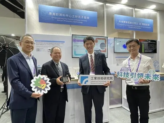
ITRI has efficiently developed Taiwan’s first 1.6 Tbps silicon photonics gentle engine module, attaining worldwide efficiency requirements. The corporate can also be collaborating with the trade to create the “Silicon Photonics Semiconductor Open Platform,” offering one-stop providers to assist corporations quickly develop silicon photonics know-how. Pictured, from left, are ASE VP, Hong Zhibin; Deputy Director of the Division of Industrial Expertise, Ministry of Financial Affairs, Zhou Chongbin; ITRI VP and Director of the Electro-Optical Analysis Institute, Zhang Shijie; and ITRI Electro-Optical Analysis Institute Group Chief, Wu Mingxian.


Leave a Reply